

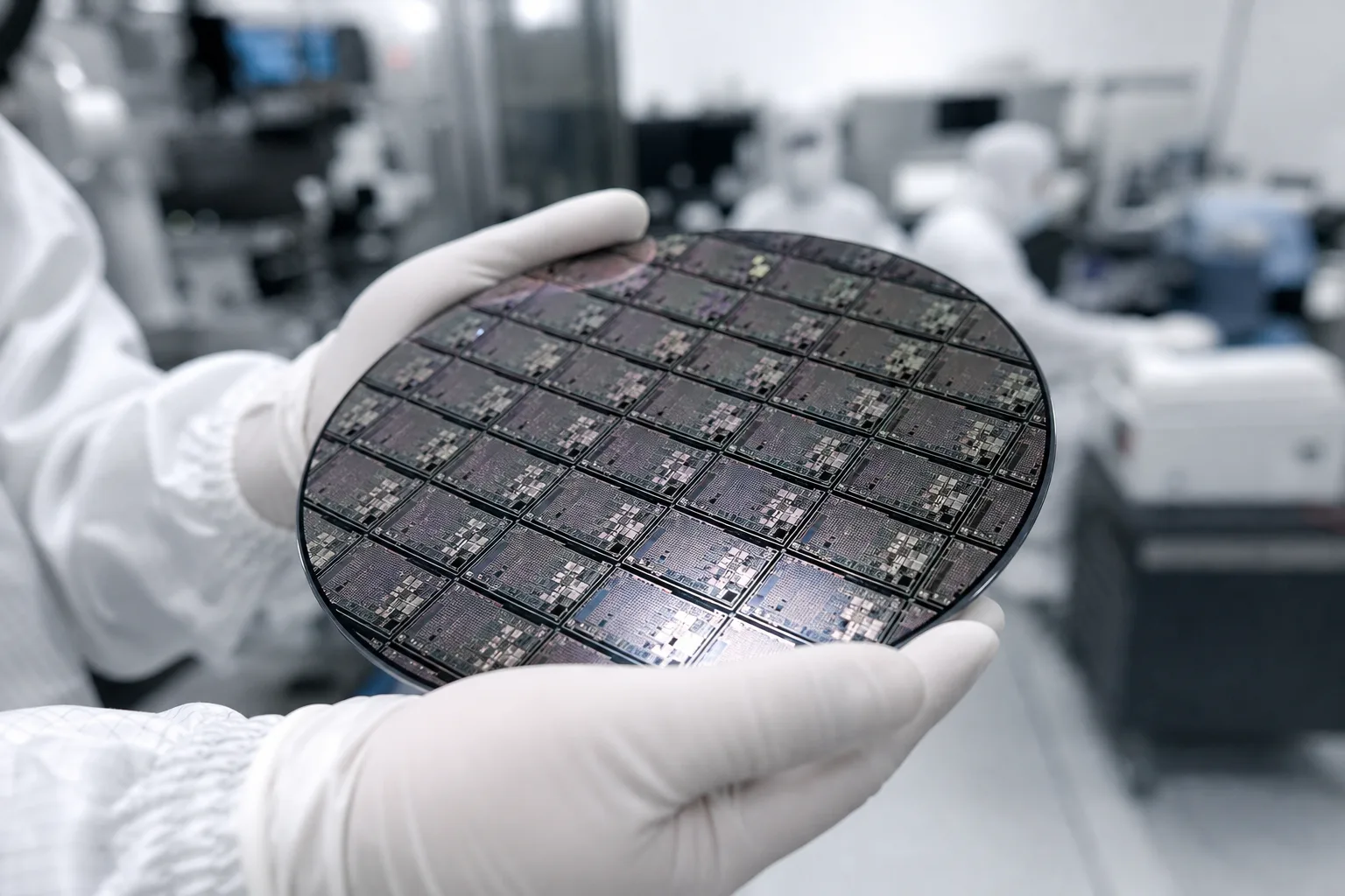
America now has its first dedicated quantum chip foundry — and the U.S. government just put a billion dollars behind it. On May 21, 2026, IBM and the Department of Commerce announced a Letter of Intent to establish Anderon, a standalone quantum wafer fabrication facility that will be headquartered in Albany, New York. The deal pairs $1 billion in CHIPS Act incentives with $1 billion in IBM cash, making it the single largest allocation within a broader $2 billion quantum package that Commerce is spreading across nine companies.
- IBM’s new quantum chip foundry Anderon receives $1B in CHIPS Act funding, matching IBM’s own $1B cash commitment.
- The quantum chip foundry will operate at 300mm wafer scale — a specification that delivers 30x faster device iteration than smaller alternatives.
- Eight other quantum companies share the remaining $1B, revealing a deliberate two-tier structure in U.S. quantum industrial policy.
- IBM CEO Arvind Krishna says Anderon could generate billions annually by the mid-2030s, comparing the moment to AI chips a decade ago.
Table of Contents
What Anderon Actually Is — and Why It Matters
Anderon isn’t just another IBM R&D facility with a fresh name. It’s designed to operate as a pure-play quantum chip foundry — meaning it will fabricate quantum chips for external customers, not exclusively for IBM’s own systems. That’s a structural shift. For the first time, quantum hardware companies won’t have to own their own fabs or depend on academic cleanrooms to manufacture serious chips at scale. They can buy time at Anderon the way classical chip designers buy time at TSMC. Having access to a dedicated quantum chip foundry on those terms is something the industry has never had before.
Initially, Anderon will focus on superconducting qubit wafers and the supporting electronics that go with them. But IBM has signaled plans to expand into other quantum modalities over time — which matters, given that the broader CHIPS quantum package is hedging across trapped-ion, photonic, and neutral-atom approaches simultaneously. A quantum chip foundry that can eventually serve multiple modalities would significantly change the economics of hardware development across the entire sector.

IBM Chairman and CEO Arvind Krishna didn’t undersell the ambition here. He compared quantum computing’s current industrial moment to where AI chips stood roughly a decade ago — before NVIDIA’s data center GPU business became a money machine — and said Anderon could be generating billions of dollars in annual revenue at strong margins by the mid-2030s. That’s a specific, confident forecast, and it tells you something about how IBM views the timing of the quantum market’s commercial inflection point.
The Quantum Chip Foundry Funding Breakdown Tells a Story
The way the $2 billion is divided across the nine recipients isn’t arbitrary. It reflects a clear government thesis about which quantum technologies are ready to be treated as industrial infrastructure and which are still science projects.
IBM’s Anderon gets $1 billion. GlobalFoundries — the only other company that could plausibly run a 300mm quantum fabrication line — gets $375 million to establish its own quantum chip foundry business. After that, the numbers drop sharply: D-Wave Quantum, Rigetti Computing, Infleqtion, Atom Computing, PsiQuantum, and Quantinuum each receive $100 million. Diraq, an Australian-founded spin qubit startup, gets $38 million.
The ratio between Anderon’s allocation and Diraq’s is roughly 26:1. Between IBM and each of the six $100 million recipients, it’s 10:1. That’s not a portfolio of equal bets — it’s a hierarchy with a clear winner at the top. The government is essentially saying: superconducting silicon is the only quantum modality that currently maps onto production-grade semiconductor manufacturing. Everything else gets venture-scale capital to keep the options open.
Commerce Secretary Howard Lutnick framed the package in predictably jobs-focused language, saying the investments would “build on our domestic industry, creating thousands of high-paying American jobs while advancing American quantum capabilities.” But the underlying industrial logic is more pointed than that talking point suggests. This is about which quantum technology gets to own the manufacturing stack — and right now, superconducting silicon is the only serious answer.
Why 300mm Wafers Change the Development Equation
The case for the quantum chip foundry running at 300mm wafer scale isn’t just about producing more chips per run. It’s about how fast you can learn.
IBM’s Director of Research Jay Gambetta, speaking at IBM Think 2026, put a specific number on it: 300mm production at Albany NanoTech delivers device output roughly 30 times faster than 200mm environments — achieved by multiplying device complexity by a factor of 10 and tripling the rate at which devices come off the line. The facility runs 24 hours a day, seven days a week, with automation that enables continuous iteration cycles. In hardware development, iteration speed is everything. It’s how you find defects, tune designs, and accumulate the empirical knowledge that eventually produces reliable, manufacturable chips.
Compare that to 200mm CMOS foundries — like the one operated by SkyWater Technology, which has positioned itself to serve government quantum programs with hands-on, custom R&D fabrication. SkyWater’s environment is genuinely valuable for early-stage research and exploratory work. But it can’t match the iteration velocity of a 300mm quantum chip foundry without a complete tooling overhaul. IBM’s early quantum chips were actually built at its own 200mm lab in Yorktown Heights — which means the company knows exactly what it’s trading up from.
GlobalFoundries’ $375 million award suggests the government wants at least a second 300mm-capable quantum chip foundry in the ecosystem. That’s smart risk management. But the structural message is clear: 300mm is production infrastructure. 200mm is research. And if you can’t access production infrastructure, your path from laboratory prototype to scalable commercial system gets very complicated very fast.
Superconducting Qubits vs. Everything Else — It’s Now a Manufacturing Question
The debate between superconducting qubits and competing approaches like trapped ions, photonics, and neutral atoms has historically been fought on physics grounds — coherence times, gate fidelity, error rates, connectivity. Those arguments aren’t going away. But the CHIPS quantum allocation reframes the competition in a different and arguably more consequential dimension: manufacturing scalability.
Superconducting qubits are fabricated on silicon wafers using processes that are closely related to classical semiconductor manufacturing. That means they can run on the same equipment, in the same fabs, with the same workforce pipelines that the broader chip industry already has. The CHIPS Act was originally designed to rebuild classical semiconductor manufacturing capacity in the U.S. — so it’s almost self-evidently logical that the quantum portion of that act would favor the quantum modality that fits most naturally into the classical fab model. A quantum chip foundry optimized for superconducting silicon is, in that sense, a natural extension of the broader CHIPS infrastructure buildout.
Trapped-ion systems, by contrast, involve manipulating individual atoms with lasers in vacuum chambers — a process that doesn’t map onto semiconductor fabrication at all. Photonic approaches have their own integration challenges. Neutral-atom systems are compelling but early. Each of these receives $100 million in CHIPS funding — enough to signal government interest, not enough to build a manufacturing base.
IBM has also built an ASIC-based control architecture for its quantum systems, designed to enable scalable fault-tolerant operation. That kind of systems-level engineering — integrating quantum processors with custom classical control electronics — is exactly the kind of work that benefits from access to a dedicated quantum chip foundry with fast iteration cycles. The companies working in trapped-ion or photonic modalities are doing genuinely important science, but they’re building against a structural disadvantage when it comes to manufacturing scale-up.
Government Equity Stakes and the Broader CHIPS Playbook
One detail that deserves more attention: the U.S. government will receive minority equity stakes in all nine companies as part of these deals. That’s the same structure Commerce applied to its agreements with Intel, rare-earths startup Vulcan Elements, and mining company MP Materials. It’s becoming a standard feature of strategic industrial policy investments, and it gives the government a financial interest in the long-term success of the companies it’s backing — not just the jobs and facilities they create in the short term.
For IBM, that means Anderon isn’t just a spinoff — it’s a partially government-owned strategic asset. That changes the political economy of the venture in ways that matter for its long-term stability. Government equity stakes create institutional constituencies that tend to protect investments from being quietly wound down when administrations change or budgets get squeezed. A quantum chip foundry with that kind of structural backing is considerably more durable than one relying solely on private capital.
What Happens If the Wrong Technology Wins?
The honest question hanging over this entire investment structure is whether concentrating half the quantum CHIPS capital in a single technology modality is a strategic masterstroke or a fragility waiting to surface. IBM’s superconducting approach is the most fabrication-ready quantum technology we have right now. It has the most publicly documented hardware progress, the largest installed base of cloud-accessible quantum systems, and the deepest integration with semiconductor manufacturing processes. The case for betting heavily on it — and on a dedicated quantum chip foundry to serve it — is real.
But quantum computing history is full of surprises. Trapped-ion systems have demonstrated some of the highest-fidelity two-qubit gates on record. Neutral-atom approaches are progressing faster than most observers expected two years ago. PsiQuantum has staked its entire existence on photonic quantum computing at silicon photonics scale — and it just received $100 million in CHIPS funding, which suggests the government hasn’t entirely written off that approach.
If one of those alternatives pulls ahead on the metrics that actually matter for fault-tolerant quantum computing — logical qubit performance, error correction overhead, the ability to run practical algorithms — the U.S. will have spent its most concentrated manufacturing investment on the runner-up. That’s a real risk. But it’s probably the right risk to take. You don’t build a quantum chip foundry around a technology that doesn’t have a manufacturing path yet. You build it around the one that does, and you use the remaining capital to keep alternatives alive. Whether that turns out to be wise policy or an expensive miscalculation will depend entirely on which physics wins — and nobody knows that yet.